Printed Circuit Boards (PCBs) are an essential component in modern electronics, serving as the backbone for a vast array of devices, from simple household gadgets to complex industrial machinery. Understanding the fundamentals of PCBs, their design, and their manufacturing processes can provide valuable insights into their significance in the technology sector.
At its core, a PCB is a flat board made of insulating material, typically fibreglass, with conductive pathways etched onto its surface. These pathways, or traces, create a circuit that connects different electronic components, such as resistors, capacitors, and microchips. The design of a PCB is crucial, as it determines how efficiently the electronic components will function together.
One of the primary advantages of using PCBs is the ability to create compact and reliable circuits. Traditional wiring methods can be cumbersome and prone to errors, especially in complex devices. PCBs streamline the manufacturing process, allowing for greater precision and reducing the likelihood of short circuits or other electrical failures. This reliability is particularly important in sectors like aerospace, medical devices, and telecommunications, where safety and performance are paramount.
The process of designing a PCB begins with a schematic diagram, which outlines the electrical connections between components. This diagram is then translated into a PCB layout using specialised software. The layout specifies the placement of components and the routing of traces, ensuring that the circuit operates as intended. Once the design is finalised, it moves to the manufacturing stage.
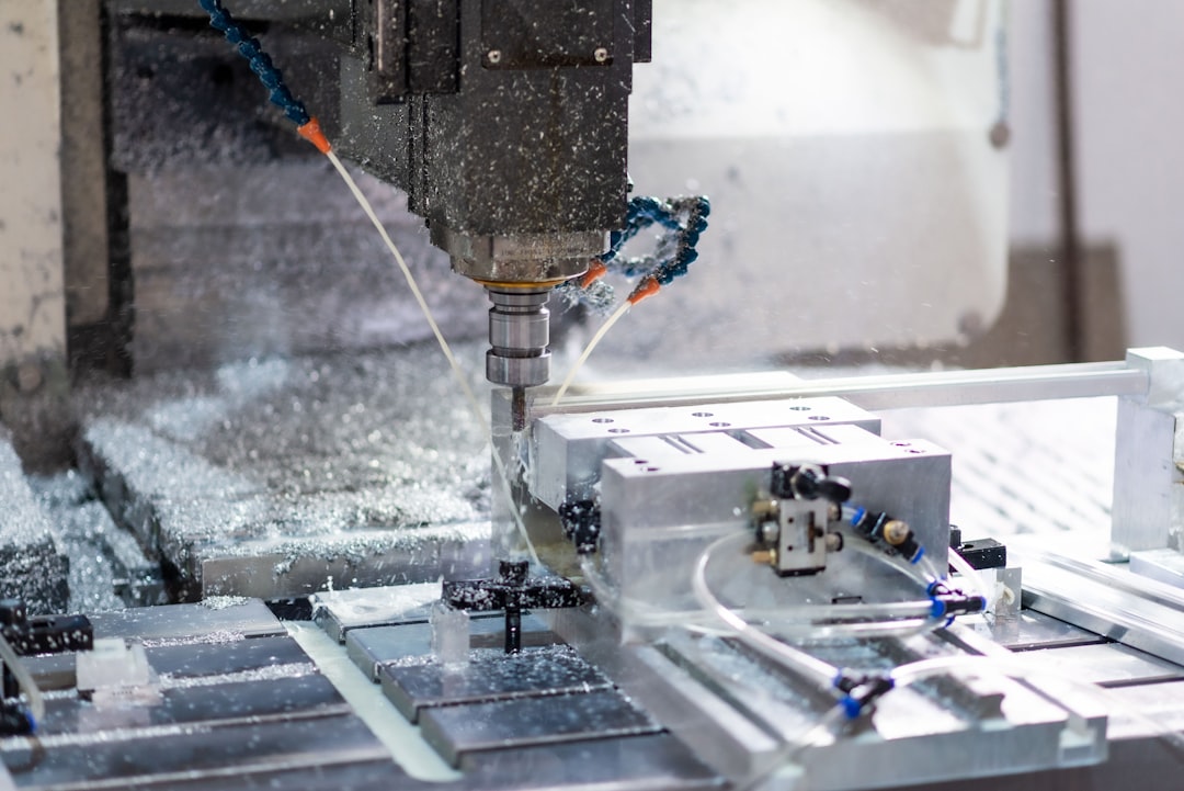
Manufacturing a PCB involves several steps. First, a substrate material is chosen, which will form the base of the board. Common materials include FR-4, a type of fibreglass, and CEM-1, a composite material. After selecting the substrate, the next step is to print the circuit design onto the board. This is typically done using a photolithographic process, where a photosensitive layer is applied, and ultraviolet light is used to transfer the circuit pattern.
After the circuit is printed, the board undergoes etching, where excess copper is removed to leave only the desired traces. Following etching, the board is drilled to create holes for component leads. These holes are then plated to ensure electrical connectivity. The final steps involve applying a protective coating and silkscreen printing labels for component identification.
For those interested in the technical aspects of PCBs, various resources are available to deepen your understanding. For instance, you can explore the principles of pcb printed circuit board design and manufacturing through online courses or textbooks. These resources often cover topics such as signal integrity, thermal management, and design for manufacturability, which are critical for creating high-quality PCBs.
Another important consideration in PCB design is the environmental impact. As technology evolves, so does the need for eco-friendly materials and processes. Manufacturers are increasingly adopting lead-free solder and recyclable materials to minimise their environmental footprint. Additionally, regulations such as the Restriction of Hazardous Substances (RoHS) directive have been implemented to limit the use of harmful substances in electronic products.
As the demand for electronics continues to grow, so does the need for innovative PCB solutions. Emerging technologies, such as flexible PCBs and embedded components, are paving the way for new applications in wearables and IoT devices. Flexible PCBs, for example, can bend and conform to different shapes, making them ideal for compact and lightweight devices.
In conclusion, understanding PCB printed circuit boards is essential for anyone involved in electronics, whether as a hobbyist or a professional. The intricate design and manufacturing processes highlight the importance of PCBs in ensuring the functionality and reliability of electronic devices. By staying informed about the latest advancements and best practices in PCB technology, individuals and businesses can continue to innovate and thrive in this rapidly evolving field. The future of electronics is undoubtedly linked to the continued development of PCBs, making them a fascinating topic of exploration.